Starting with efinity IDE
To run your code on the FPGA, follow these steps:
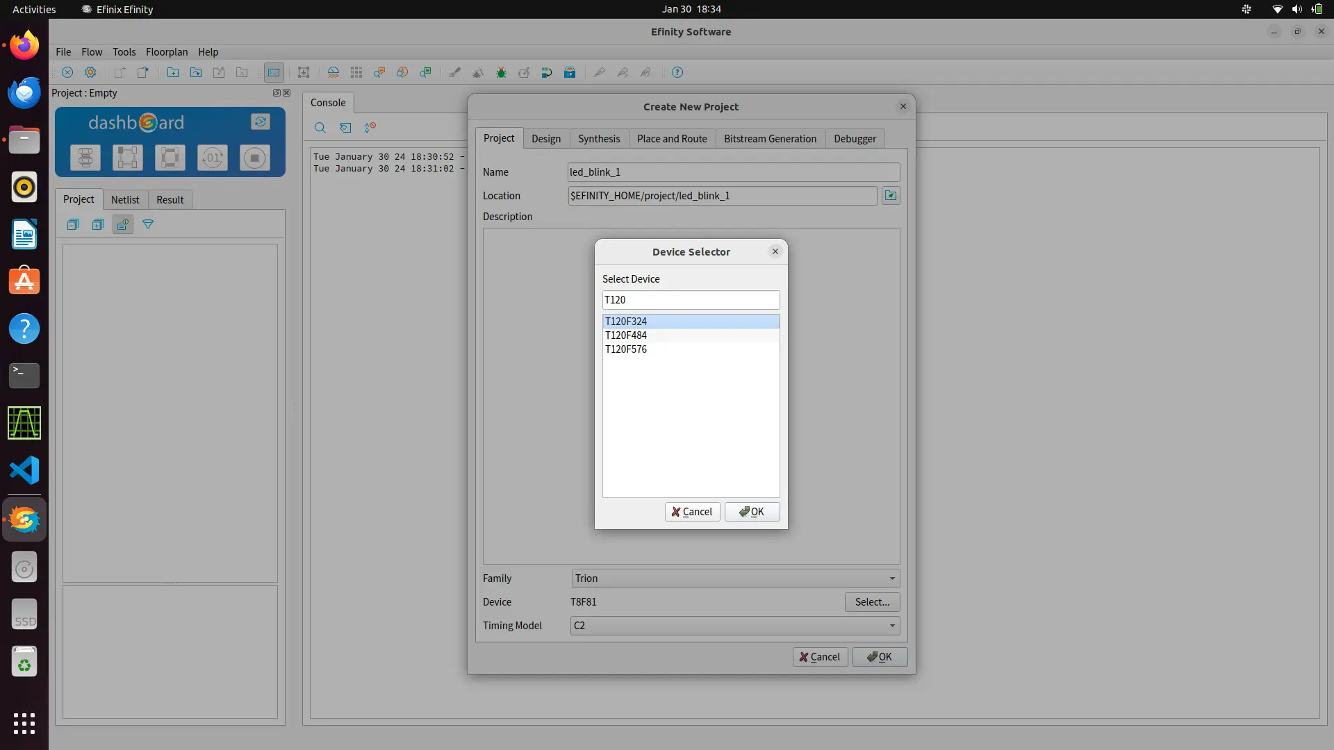
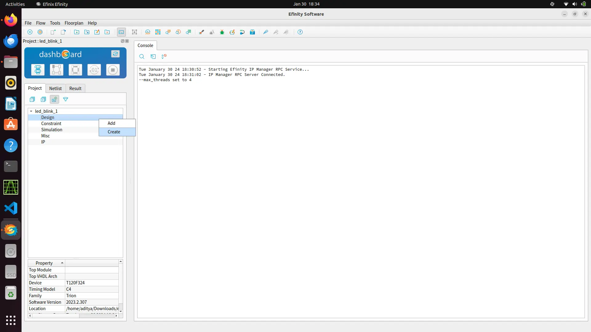
After starting the IDE click on files and create a project. Write your project name and select trion family and fpga T120F324. Timing model C4 would be automatically selected.
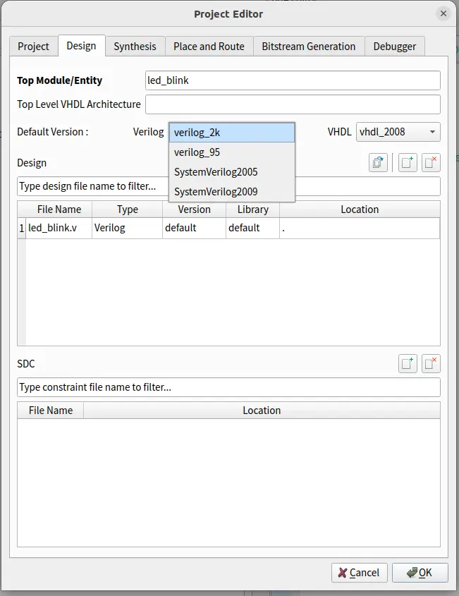
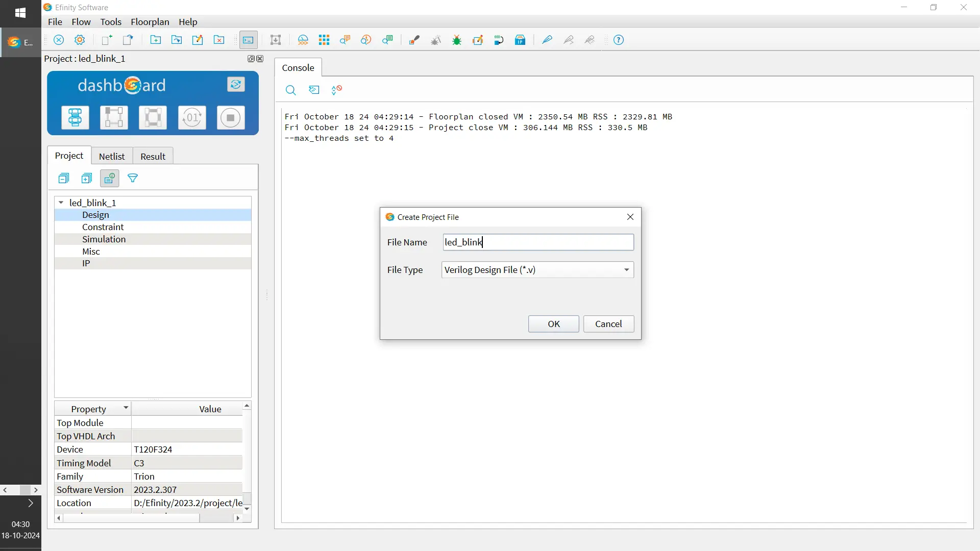
In the design tab you can select your prefereable HDL. Verilog ,systemverilog and VHDL are supported. Default is verilog. You can also add your rtl code while the creation of project and specify the top module.
In Dashboard , you can add/create your verilog files by right-clicking on design tab under your project.
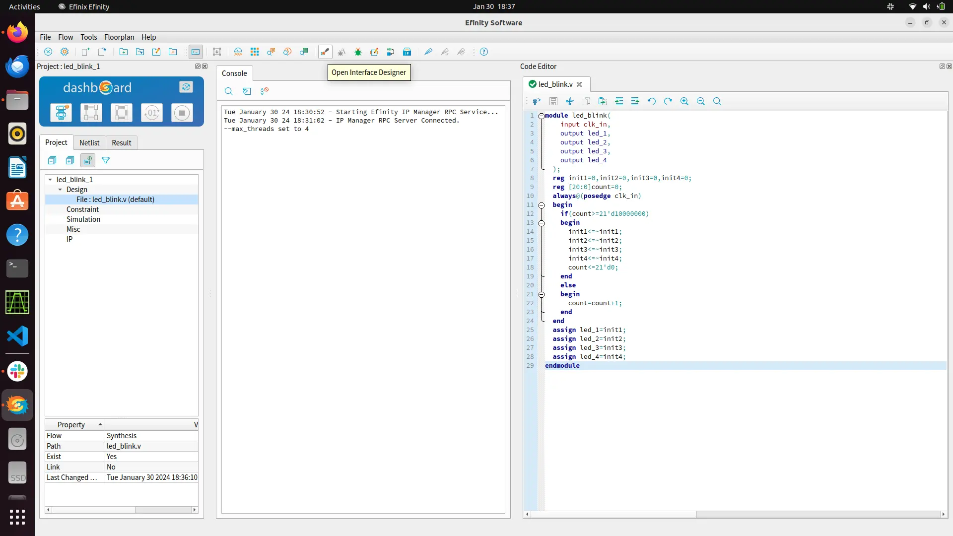
Default gedit editor will pop-up on right side on which you can write your code. Save the code. led blinking demo code.
Now you need to open inferace designer to map your signals to the fpga boards GPIO.
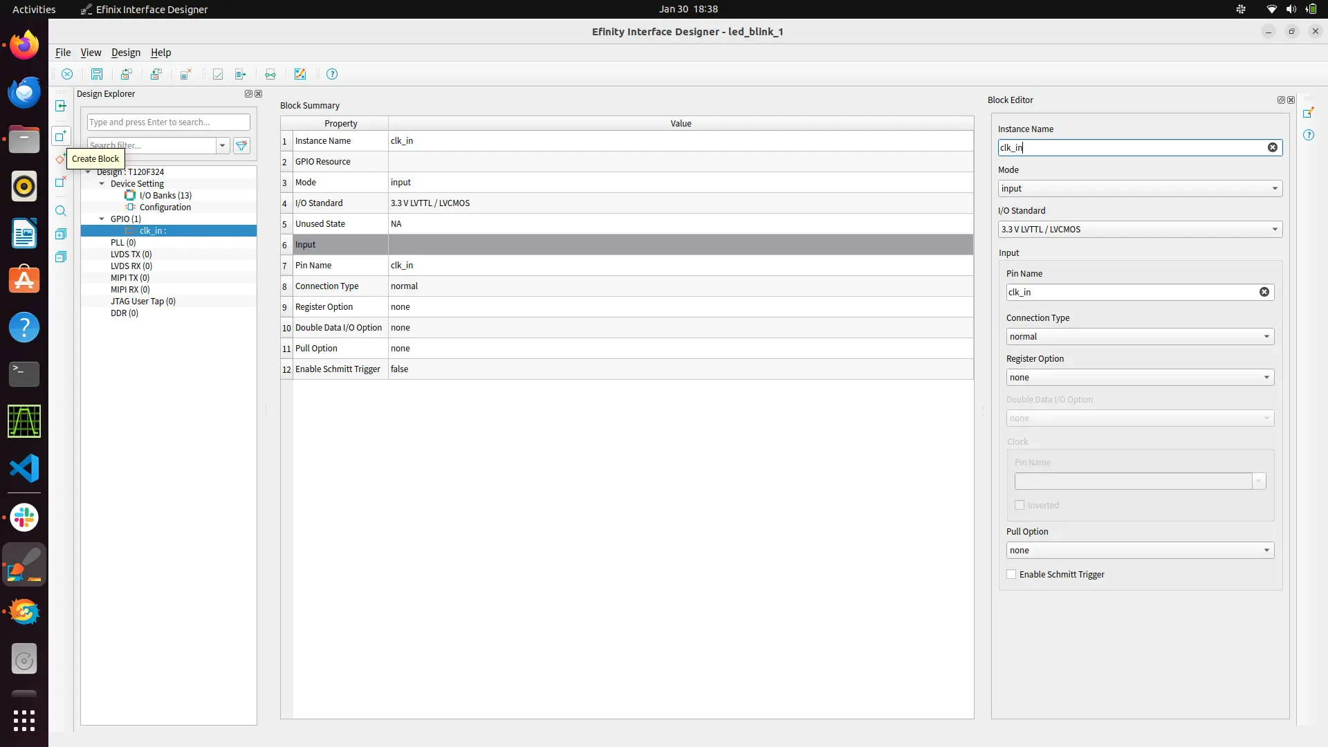
Create a gpio block and configure your pins as input/output mode as per your design
Setting PLL
The FPGA have crystall oscillators which can give frequency upto 74.5Mhz. You can use this crystall oscillators as source clock and generate the desired frequency via PLL.

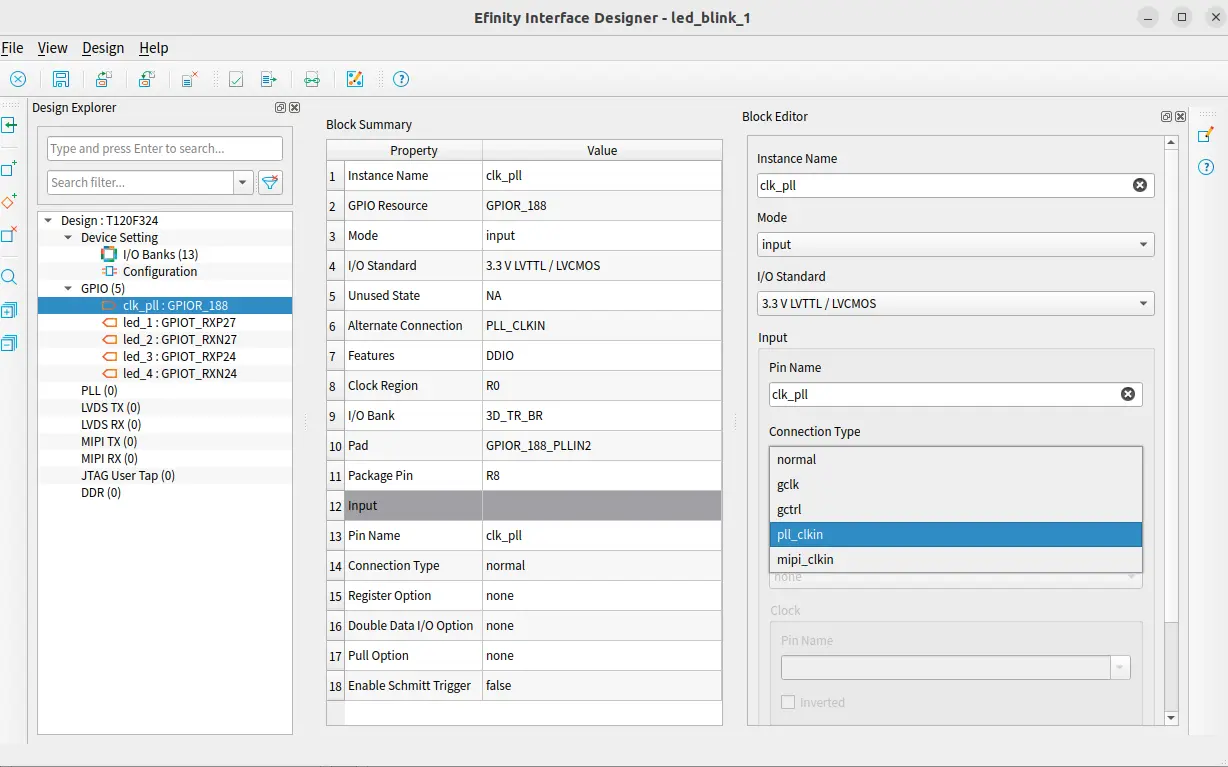
While creating the gpio block for source clock you need to change its connection type from normal to PLL_CLK_IN. and give this pin any crystall oscillator in resouce assigner.
For PLL you need to create a PLL block as done for gpio. Select the source clk. The selected source clk instance name would be shown below once selected.
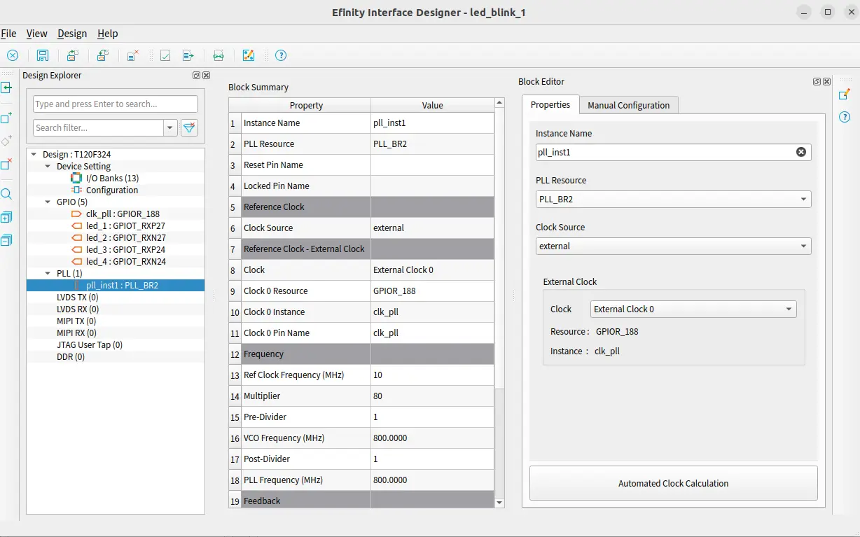
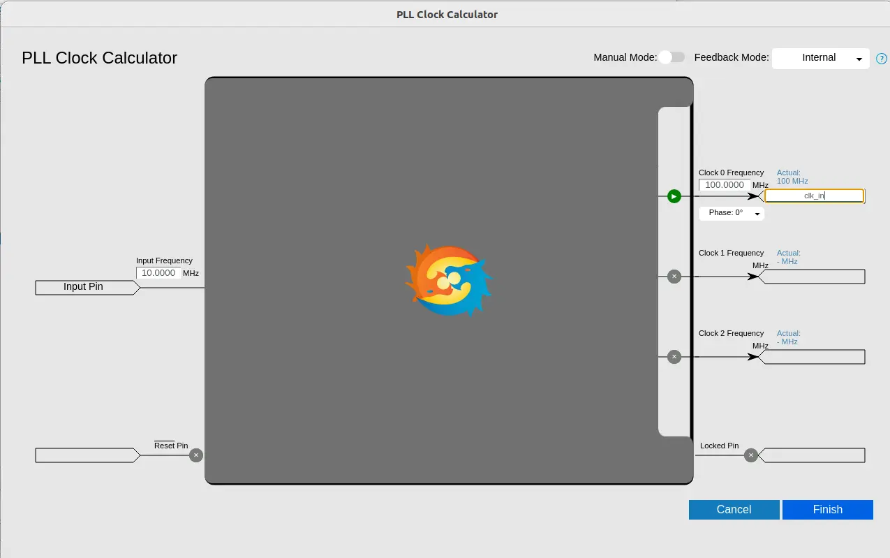
Here both automated calculation and manual calculation options are available for setting the PLL. You can choose any of these as per your convenience. Here you have to mention your actual clock input which will be fed in the design.
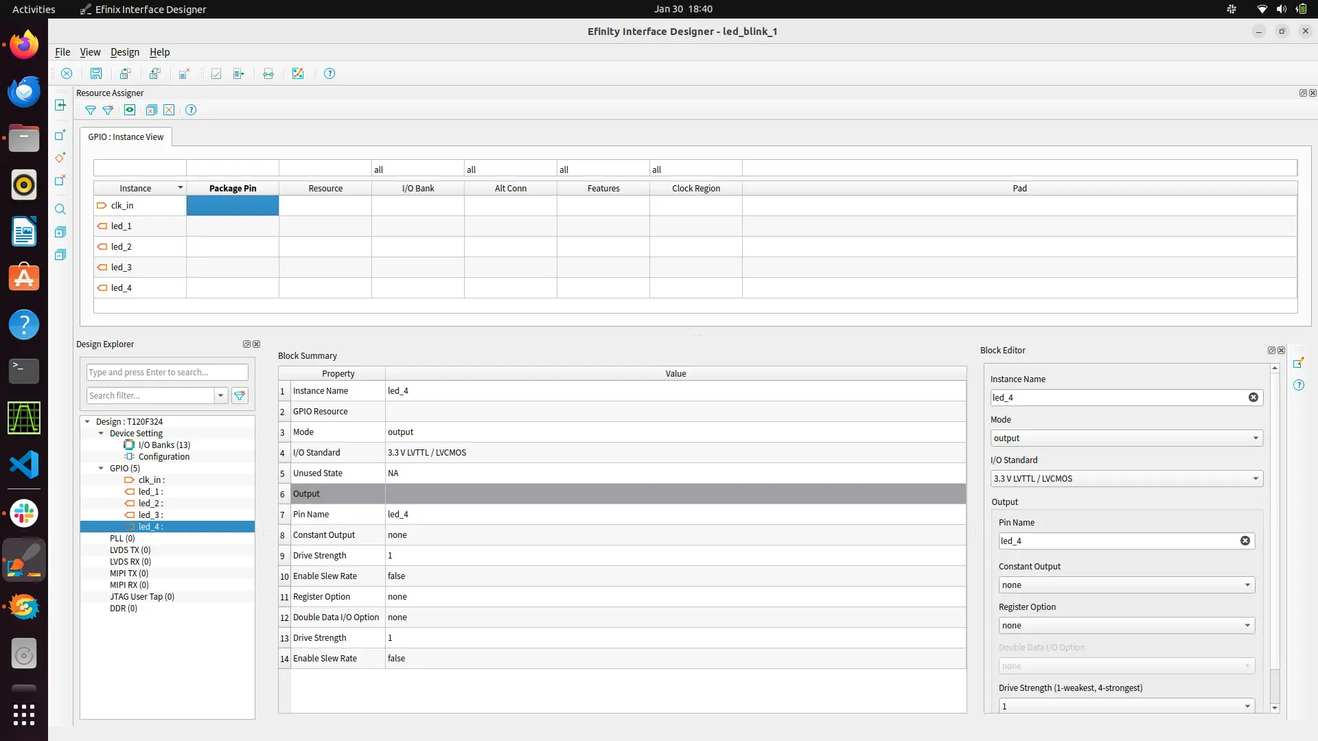
Navigate to the resource assigner to map the pins on board. You can refer to pinout guide for mapping. By entering the package pin the rest of the colums would be to auto-fill
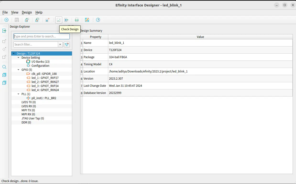
Now check for design issue. It throws error if there’s any error in mapping the pins. Now save the interface design.
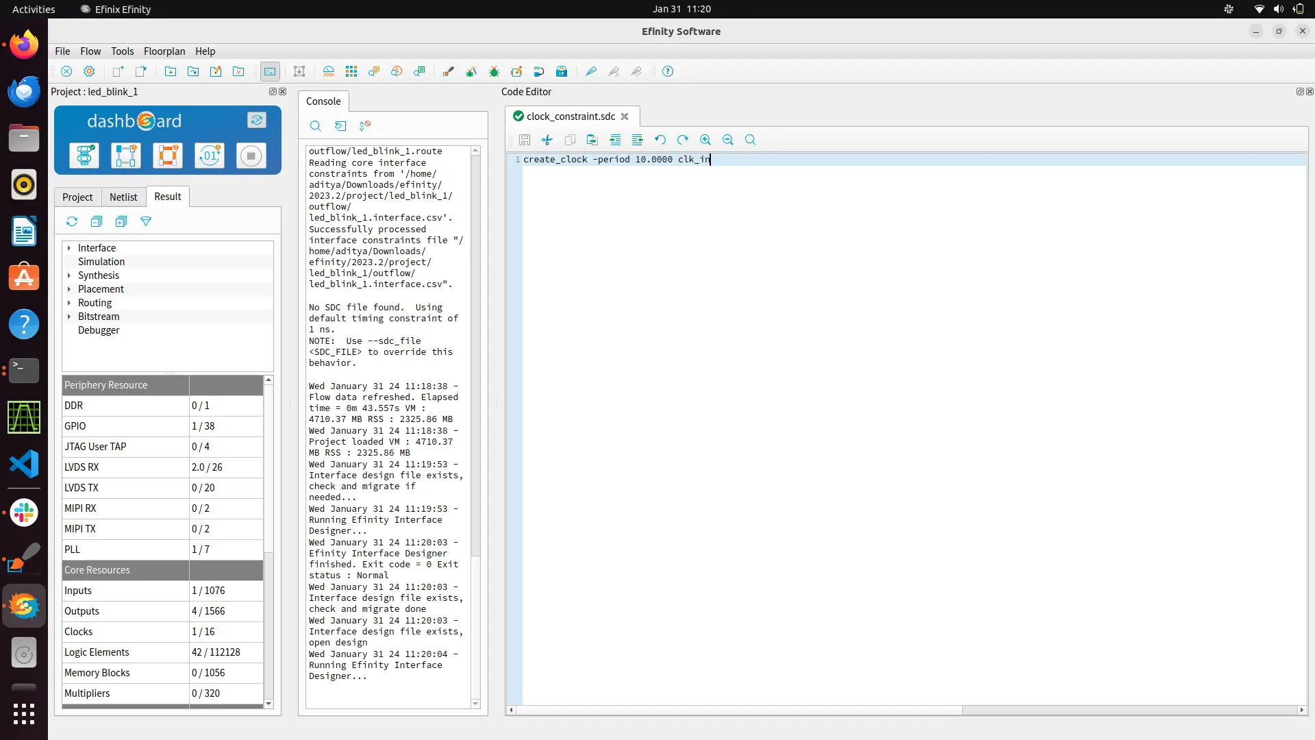
You can also give constrains for your design by creating a constrain file with .sdc extension.
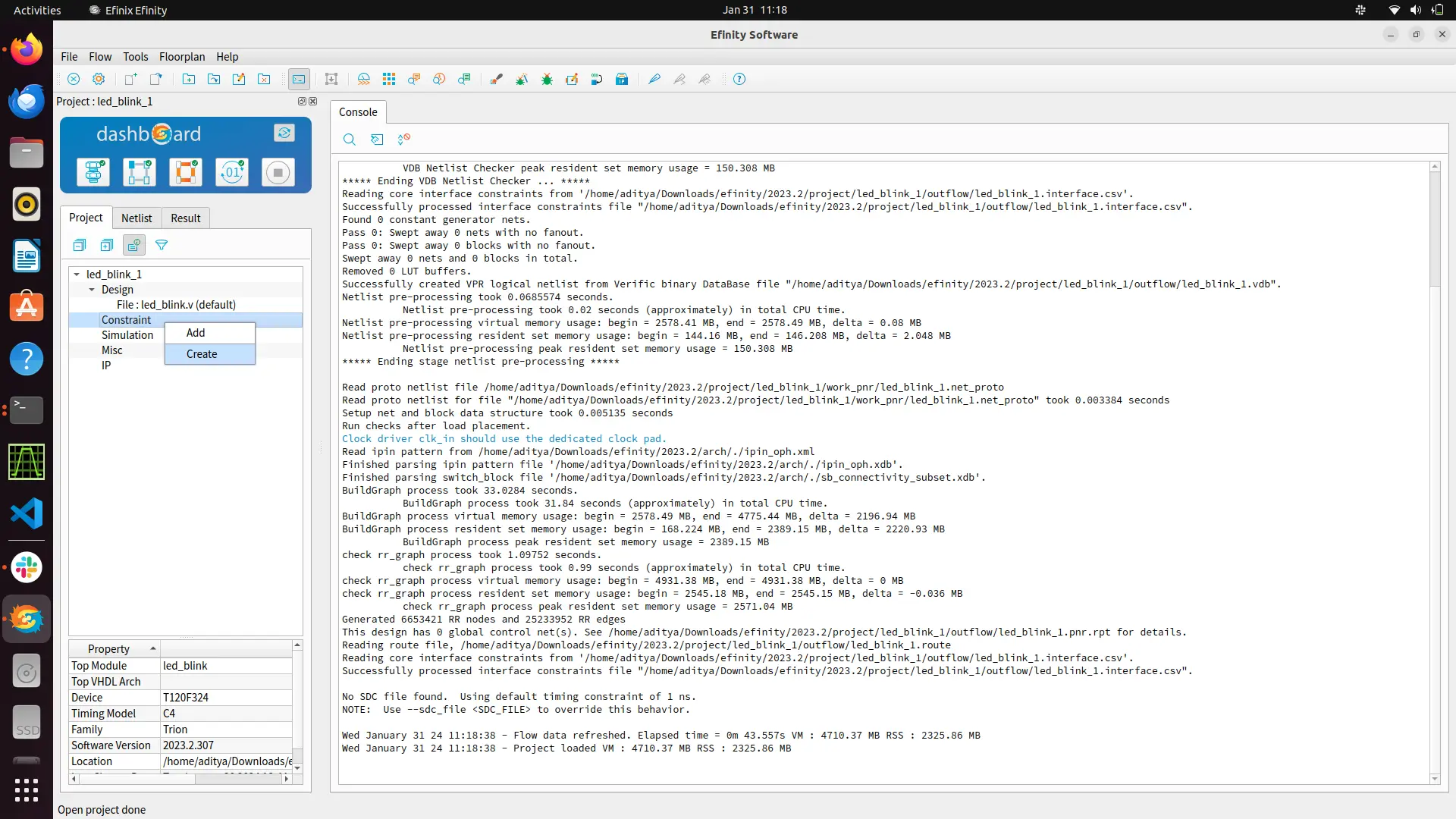
Here you can mention your virtual clock or mention the input/output delay. According to the constrain the software will perform the placement and routing to meet the desired perfomance.
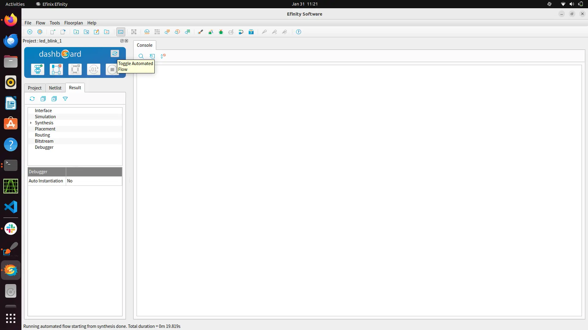
Now just press synthesis option to run your entire flow. By default it will run the entire flow of synthesis, placement ,routing and bitsream generation. You can toggle it off for running one flow at time. After running the entire flow in project directory and outflow/ directory will generated containing all the generated files at each step.
Now follow the steps on Vaaman FPGA Programming to dump your generated bitstream on FPGA.
How to use Debugger
The Efinity software features a hardware Debugger, facilitating signal probing in FPGA designs through the JTAG interface. The Debugger encompasses two debug cores:
Configure Virtual I/O (vio) cores using a manual flow and the Profile Editor.
Configure Logic Analyzer (la) cores either through a manual flow or the automated flow of the Debug Wizard.
The subsequent sections provide detailed guidance on both the automated and manual flows.
Automated debugger
Create a Debug Profile:
Open the project.
Synthesize the design.
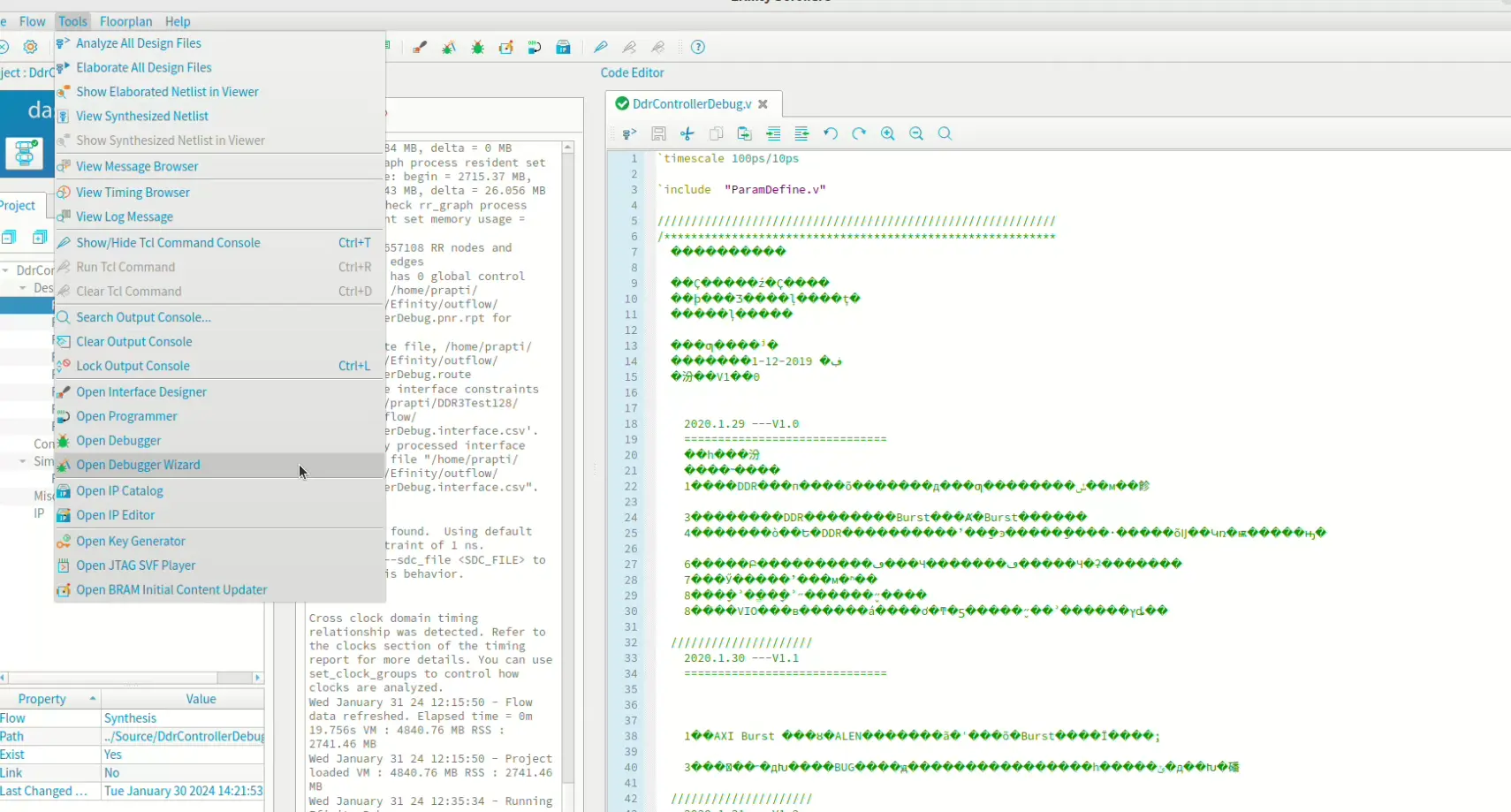
Launch the Debug Wizard by clicking its icon in the main icon bar.
Choose “Elaborated Netlist” or “Post-Map” in the Signals from list.
Select led and counter buses from the left list and move them to the right using the >> button.
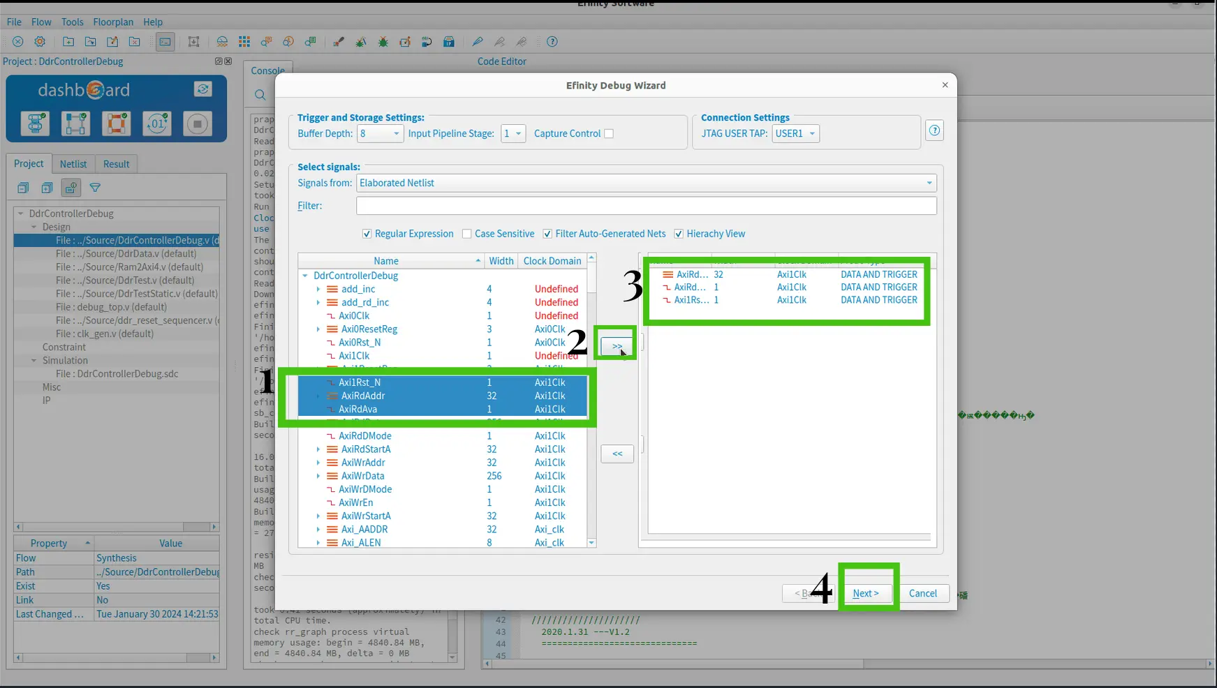
Keep the Probe Type as default, DATA AND TRIGGER.
Proceed to the next step. The wizard generates a debug profile.
Ensure “Auto Instantiation” is enabled to integrate the debug profile into your project. Click Finish.
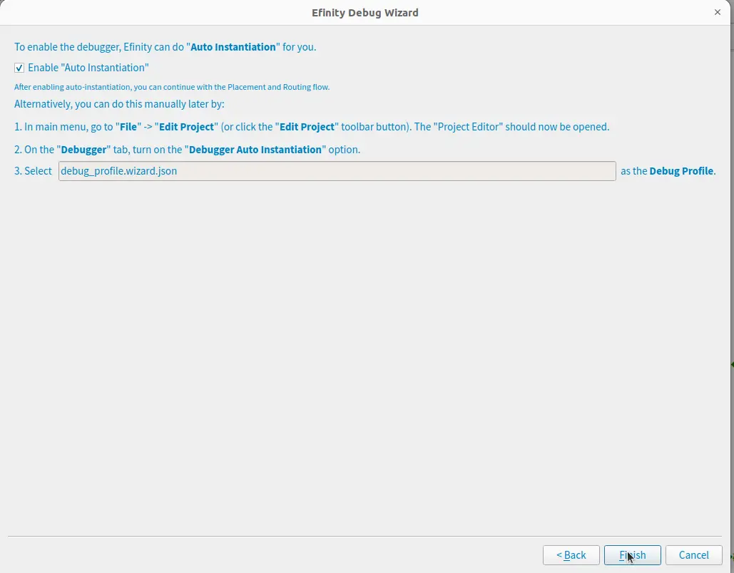
The software prompts for recompilation. Click OK.
Perform a full compile.
Programming FPGA for debugger
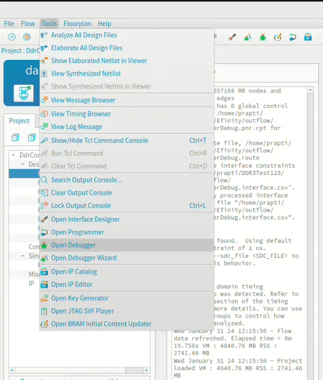
Launch the Debugger by choosing Tools > Open Debugger.
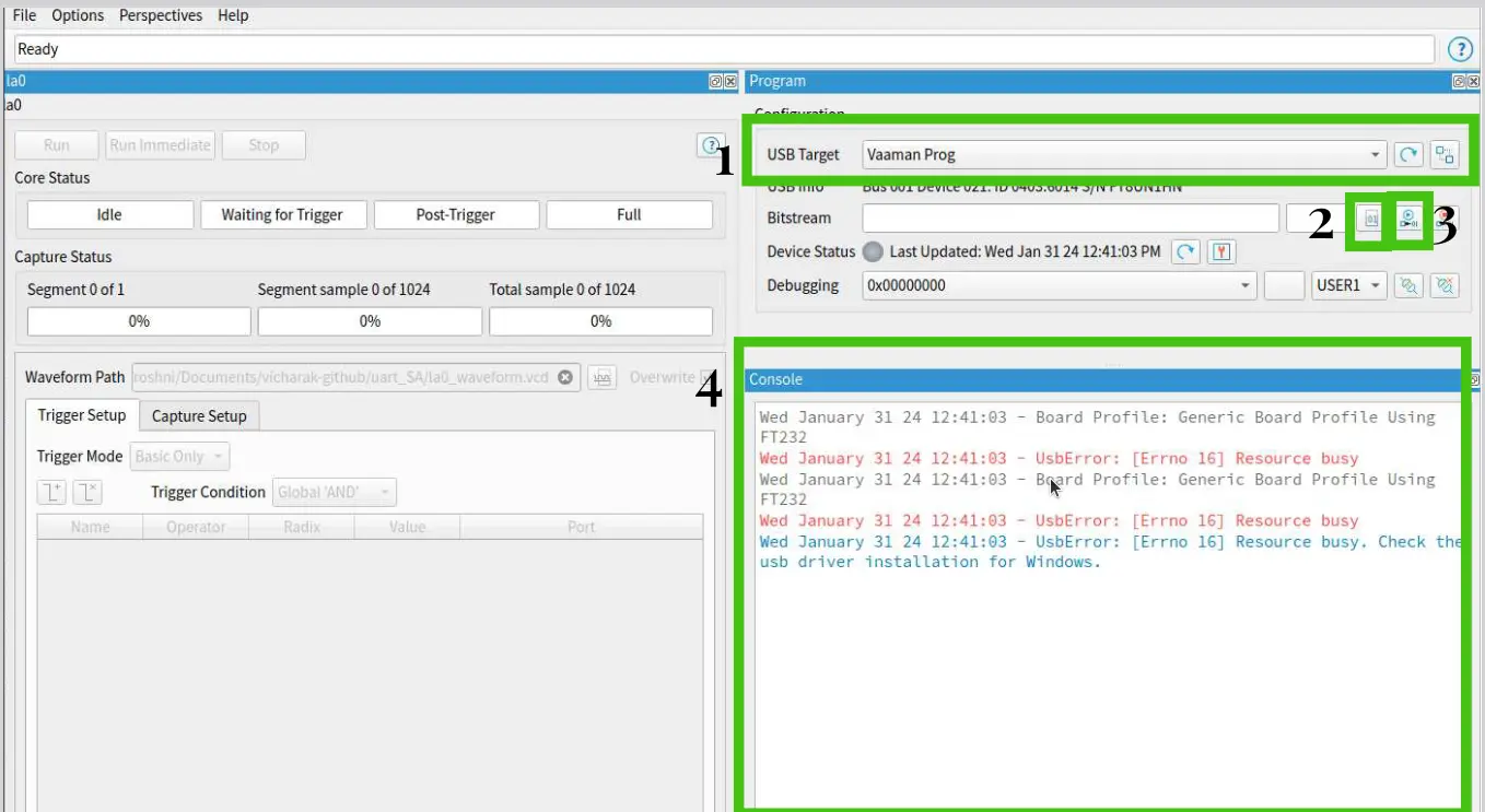
Ensure the Board is recognized as the USB Target. If not, connect the board and click Refresh USB Targets.
Click the Select Image File button.
Navigate to the outflow directory and choose bitstream file.
Click Start Programming. The console will display programming messages.
Observing Probed Signals in Debugger
Initiate Debugger connection.
In Trigger Setup tab, add desired nets.
Specify trigger conditions (e.g., value).
Start Debugger to capture data upon trigger.
Upon completion, GTKWave opens automatically to display waveform.
Disconnect Debugger to halt operation.
Manual Debugger
Create Debugger Profile
To configure Virtual I/O and Logic Analyzer debug cores in a profile:
Open the project.
Launch the Debugger via Tools > Open Debugger. Since no debug profile exists, the Profile Editor perspective opens.
Add a Virtual I/O core (VIO) using Add Debug Core > Virtual I/O. Configure Probes(input) and source(output) signals as specified (i.e name and width).
Add a Logic Analyzer core (LA) via Add Debug Core > Logic Analyzer. Configure probes to capture signals matching VIO settings. the vio0 tab to view captured data in the Value fields.
Generate Debug RTL to create necessary debug files.
Open debug_top.v and rename “edb_top” as “edb_top_manual.”
Close the debugger.
Add Debug core in your project
To integrate debug code into your project and compile it:
Open the Efinity main window and go to the Project tab.
In the Interface Designer, add the JTAG User Tap block, configure it, and generate SDC constraints.
Close the Interface Designer.
Modify design file by uncommenting specific lines to enable debug code and instantiate debug_top module.
Save your changes.
Compile the design.
Programm the FPGA
To program the FPGA:
Open Debugger by choosing Tools > Open Debugger.
Confirm the Trion T20 Development Board is recognized as the USB Target; refresh if necessary.
Select the FPGA configuration file (bitstream) from the outflow directory using the Select Image File button.
Initiate programming by clicking Start Programming, and monitor programming messages in the console.
Run the Debugger
Observing Probed Signals in Debugger:
Connect Debugger and navigate to the la0 tab for trigger setup.
Add the desire trigger condition.
If want the change the vio0 values and Run the debugger.
Then its wait for thrigger, after applying trigger open the GTKWave for checking the debug signal.
Disconnect Debugger to stop capturing data.